- 您现在的位置:买卖IC网 > Sheet目录311 > AS1112C-BQFT (ams)IC DRIVER LED 16CHAN 32-TQFN
�� �
�
�AS1112�
�Datasheet� -� D� e� t� a� i� l� e� d� D� e� s� c� r� i� p� t� i� o� n�
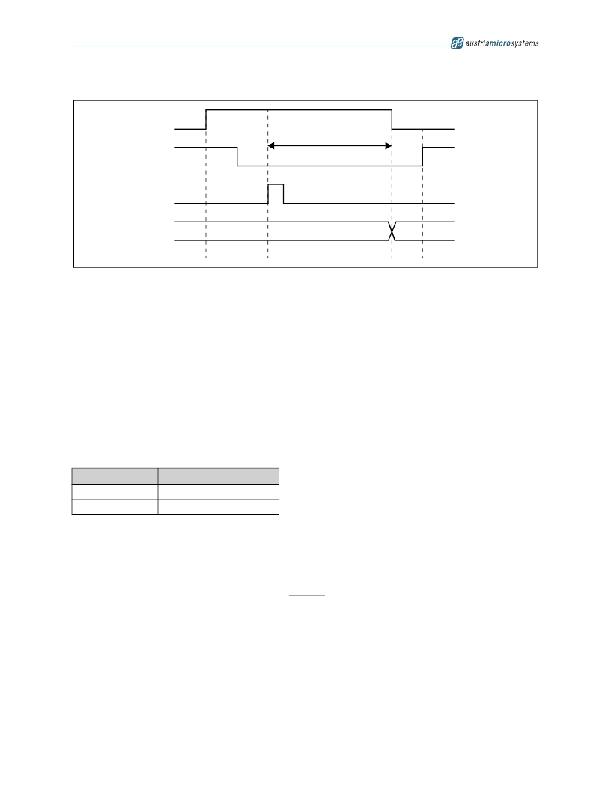
�Figure� 10.� Error� Detection� Timing� (GS=FFFF� HEX� ,� DC=3F� HEX� )�
�LD�
�>1μs�
�OEN�
�GSCLK�
�SID�
�Error�
�Detection�
�Start�
�LOD� n� ,� LSD� n�
�LOD� n+1� ,� LSD� n+1�
�Error�
�Detection�
�End�
�Note:� The� rising� edge� of� LD� latches� new� data� into� the� internal� registers� depending� on� the� logic� level� of� the� pin� MODE.� If� the� pin� MODE� is� tied�
�GND,� the� greyscale� registers� are� updated.� If� the� pin� MODE� is� tied� to� V� CC� ,� the� dot� correction� registers� are� updated.�
�Delay� Between� Outputs� (only� for� AS1112� and� AS1112B)�
�The� AS1112� uses� graduated� delay� circuits� between� OUT� n� outputs.� These� circuits� are� contained� in� the� constant-current� driver� block� of� the�
�AS1112� (see� Figure� 1� on� page� 1)� .� The� average-delay� time� is� 30ns� (typ).�
�The� maximum� delay� is� 450ns� (typ)� from� OUT0� to� OUT15.� The� delay� scheme� works� by� switching� on� and� switching� off� each� output� channel.� Thus�
�the� on/off� time� of� each� channel� is� the� same� regardless� of� the� delay.� These� delays� prevent� large� inrush� currents� and� switching� noise� that� can�
�reduce� bypass� capacitance� when� the� outputs� are� switched� on.�
�OUT� n� Enable�
�All� OUT� n� channels� can� be� collectively� switched� off� with� one� signal.� When� OEN� is� set� to� 1,� all� OUT� n� channels� are� disabled,� regardless� of� the�
�device� logic� operations.� The� greyscale� counter� is� also� reset� when� OEN� is� set� to� 1.�
�When� OEN� is� set� to� 0,� all� OUT� n� channels� are� in� normal� operation.�
�Table� 9.� Pin� OEN� Truth� Table�
�OEN�
�0�
�1�
�OUT0:OUT15�
�Normal� Operation�
�Disabled�
�Setting� Maximum� Channel� Current�
�The� maximum� output� current� per� channel� is� programmed� by� a� single� resistor,� R� IREF� ,� which� is� placed� between� pin� I� REF� and� GND.� The� voltage�
�on� pin� I� REF� is� set� by� an� internal� band� gap� V� IREF� (1.24V� typ).� The� maximum� channel� current� is� equivalent� to� the� current� flowing� through� R� IREF�
�multiplied� by� a� factor� of� 31.5.� The� maximum� output� current� is� calculated� as:�
�I� MAX� =�
�V� IREF�
�x� 31.5�
�(EQ� 1)�
�R� IREF�
�Where:�
�V� IREF� =� 1.24V;�
�R� IREF� =� User-selected� external� resistor.�
�Figure� 7� on� page� 7� shows� the� maximum� output� current� I� OUT� versus� R� IREF� ,� where� R� IREF� is� the� value� of� the� resistor� between� I� REF� terminal� to�
�GND,� and� I� OUT� is� the� constant� output� current� of� OUT0:OUT15.�
�www.austriamicrosystems.com/LED-Driver-ICs/AS1112�
�Revision� 1.13�
�10� -� 19�
�发布紧急采购,3分钟左右您将得到回复。
相关PDF资料
AS1113-BSST
IC DRIVER LED 16-CHAN 24-SSOP
AS1117-BQFT
IC DRIVER 64LED MOBILE 24-TQFN
AS1118-BQFT
IC DRIVER 64LED W/DELAY 24-TQFN
AS1121B-BQFT
IC DRIVER 16-CH 32-TQFN
AS1122B-BQFT
IC LED DVR 12-CH 24-TQFN
AS1123-BTST
IC LED DVR 16-CH 40MA 24-QSOP
AS1390A-ZQFT
IC BOOST CTLR/BUCK CONV 20-QFN
AS212-L
SOCKET 12V AUTO SAFETY CAP MNT
相关代理商/技术参数
AS1112-EB
制造商:ams 功能描述:AS1112 Evaluation Board
AS1112-XXX-I-A1-D
制造商:未知厂家 制造商全称:未知厂家 功能描述:Analog Filter
AS1112-XXX-I-A1-S
制造商:未知厂家 制造商全称:未知厂家 功能描述:Analog Filter
AS1112-XXX-I-A2-D
制造商:未知厂家 制造商全称:未知厂家 功能描述:Analog Filter
AS1112-XXX-I-A2-S
制造商:未知厂家 制造商全称:未知厂家 功能描述:Analog Filter
AS1112-XXX-I-A3-D
制造商:未知厂家 制造商全称:未知厂家 功能描述:Analog Filter
AS1112-XXX-I-A3-S
制造商:未知厂家 制造商全称:未知厂家 功能描述:Analog Filter
AS1112-XXX-I-L-A1-D
制造商:未知厂家 制造商全称:未知厂家 功能描述:Analog Filter